(Ultra)Wide Bandgap Materials and Devices Laboratory
We pursue synthesis, advanced characterization, and engineering of wide and ultrawide bandgap (UWBG) semiconductors and heterostructures, along with device design, modeling, and fabrication, to enable advances in high-power, high-frequency electronic and ultraviolet optoelectronic applications. Our work also extends to understanding how these materials and devices operate under extreme environments, including high temperature, radiation, and nuclear conditions, where long-term resilience is critical. Below are some of the research domains that are of great interest to our research group.
Material Synthesis and Processing
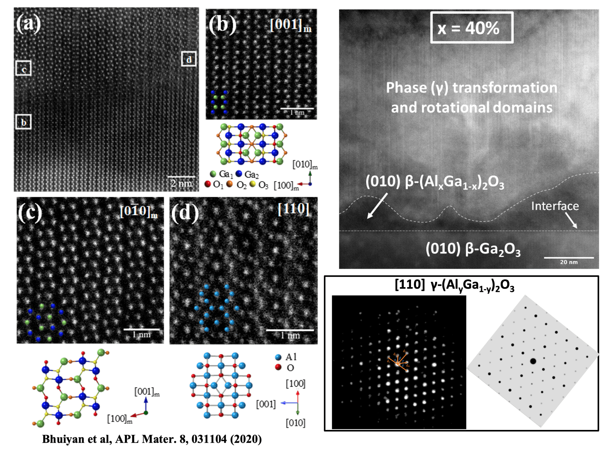
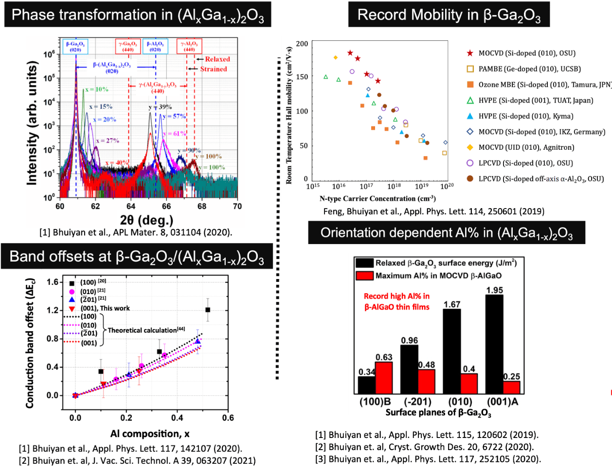
We are developing new growth and processing methods for Ga₂O₃ and related ultrawide bandgap (UWBG) semiconductors using chemical vapor deposition (CVD) techniques. Our efforts include in-situ etching, selective area growth, and regrowth to achieve high-quality films and anisotropic structures. By engineering crystal quality, doping, interfaces, and defect populations, we create high-quality materials designed for reliable performance under high-power and extreme environmental conditions.
Device Design and Fabrication
We design, fabricate, and study devices based on ultrawide bandgap (UWBG) materials, guided by TCAD simulations and modeling that probe electric fields, carrier transport, breakdown phenomena, and thermal behavior. By linking materials growth to device functionality, we explore the fundamental physical limits of UWBG semiconductors and develop architectures optimized for high-power and high-frequency electronics.
Radiation and Nuclear Environment Electronics
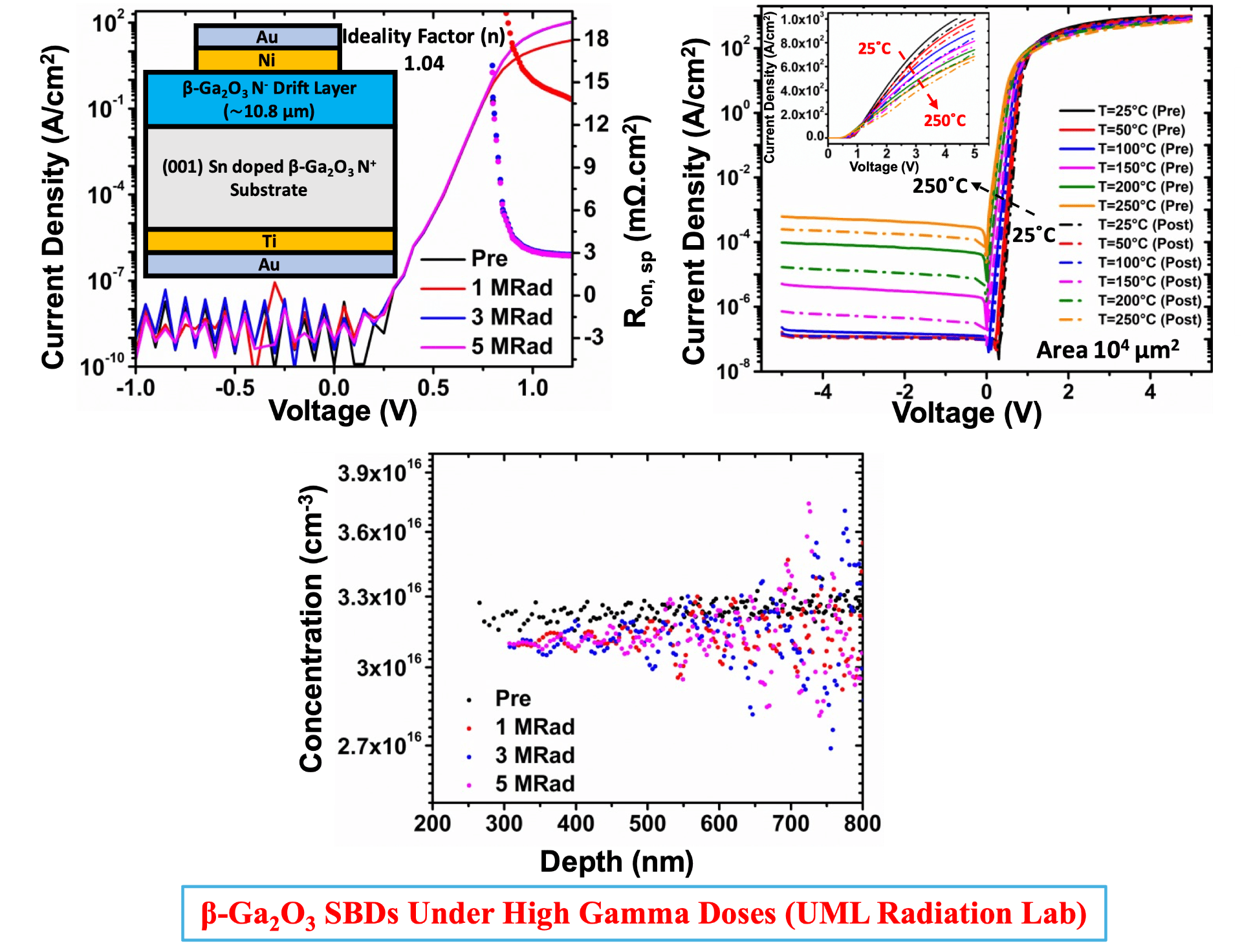
A major thrust of our work is understanding and mitigating the effects of gamma rays, neutrons, protons, and heavy ions on ultrawide bandgap (UWBG) semiconductors and devices. We study how radiation introduces and evolves defects, alters carrier transport, and impacts device reliability. These insights directly inform the development of radiation-hardened materials and devices for nuclear energy systems, space electronics, and defense applications.
Superconductor–Semiconductor Heterostructures
We are exploring hybrid systems that integrate superconductors with wide and ultrawide bandgap semiconductors to enable next-generation cryogenic, quantum, and high-performance electronic platforms. Our research spans thin-film synthesis, interface engineering, and device integration to advance reliable and scalable technologies for future electronics.
Thermal Management for Harsh Conditions
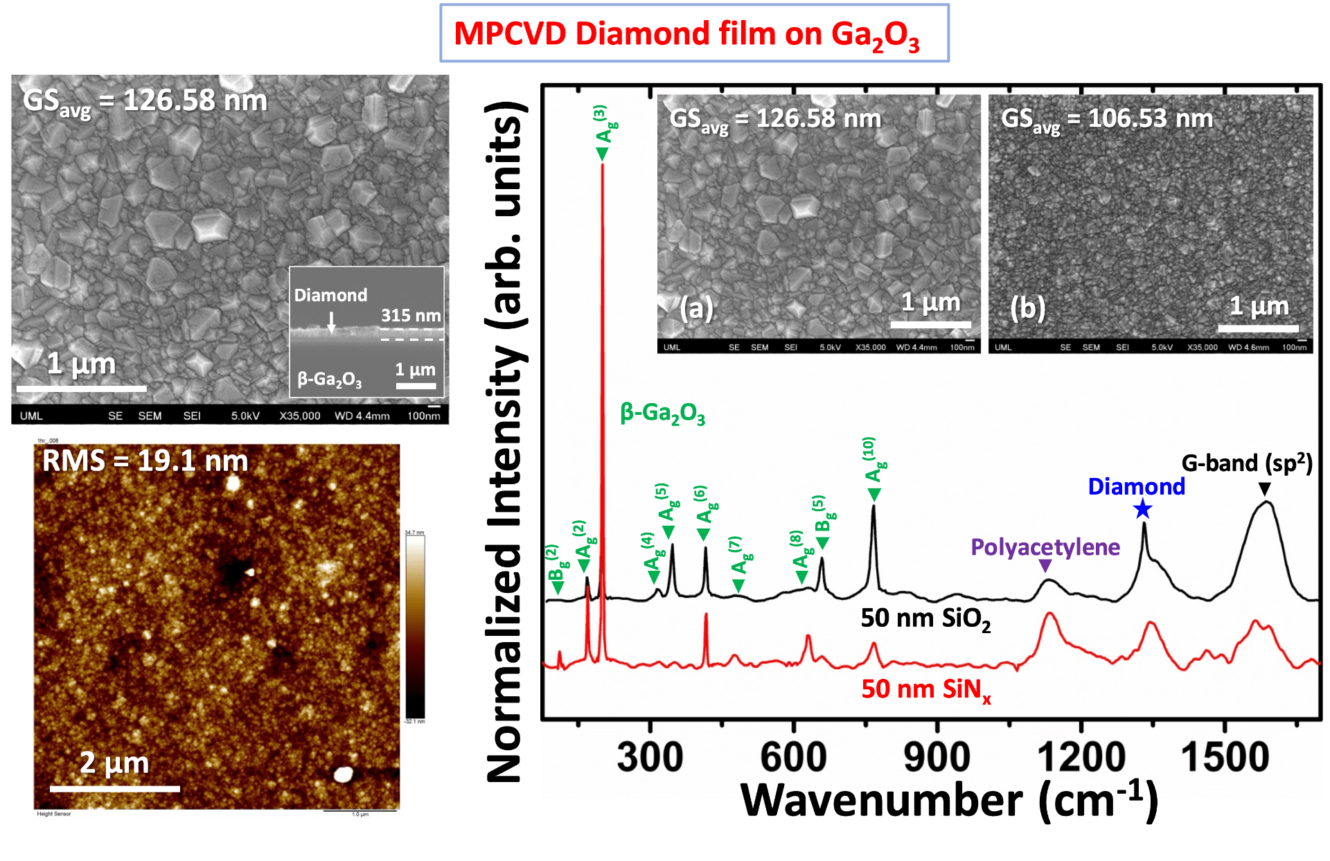
Heat is one of the most severe constraints on ultrawide bandgap (UWBG) device performance. We are pursuing strategies that integrate polycrystalline diamond and other thermally conductive materials to lower thermal resistance and improve stability under high-power operation. These efforts are critical for ensuring robust device performance in nuclear and aerospace environments, where cooling options are limited.