Facilities and Resources
(Ultra)Wide Bandgap Materials and Devices Laboratory
Our lab is located at UMass Lowell North campus, Ball Hall 308. We combine dedicated in-lab tools with shared university and partner facilities that support materials growth, microscopy and spectroscopy, nanofabrication, electrical testing, and radiation exposure studies.
Materials Growth
Saleh and Ahmed performing CVD deposition of Ga₂O₃ at Ball Hall 308.
Low-Pressure Chemical Vapor Deposition (LPCVD)
Epitaxial growth of Ga₂O₃ and related oxides, including doped films and process exploration for scalable, high-quality layers.
Halide Vapor Phase Epitaxy (HVPE)
HVPE growth facility for thick, low-doped Ga₂O₃ drift layers for vertical device development.
Seki Technotron MPCVD system for diamond growth.
Microwave Plasma Chemical Vapor Deposition (MPCVD) system for Diamond Growth
The Seki Technotron MPCVD reactor enables synthesis of high-quality polycrystalline and nanocrystalline diamond films. The system provides stable plasma-assisted growth with precise gas-phase control, supporting uniform nucleation and scalable diamond deposition for advanced device platforms.
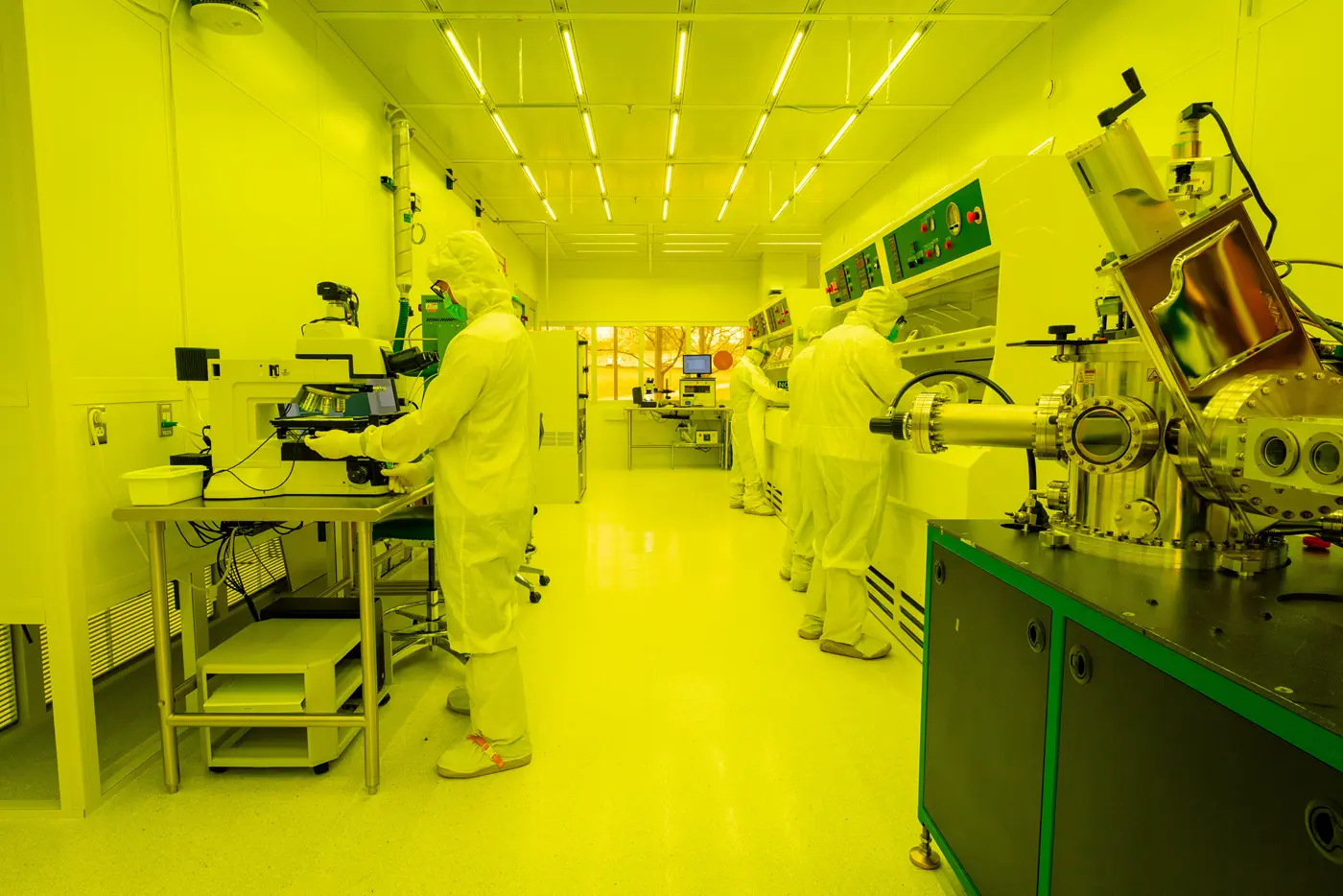
Nanofabrication
UMass Lowell Nanofabrication Laboratory, North Campus.
Materials Characterization
Microscopy Core Laboratory (MCL), UMass Lowell Core Research Facilities.
Electrical and Defect Characterization
Temperature-Dependent Hall System
Ecopia HMS-5300 system for the measurements of carrier concentration, mobility, Hall coefficient, resistivity, conductivity, and magnetoresistance (77–350 K), located in Bhuiyan Lab at Ball Hall 308.
Semiconductor Parameter Analyzer and Probe Station
Keithley 4200A-SCS with SEMIPROBE system for I–V and C–V testing (25–250 °C).
Deep Level Transient Spectroscopy (DLTS)
DLTS capability for deep-level defect analysis in semiconductors, located in Bhuiyan Lab at Ball Hall 308.
Radiation Laboratory
The UMass Lowell Radiation Laboratory houses a 1 MW swimming-pool–type nuclear research reactor and a 5.5 MV Pulsed Van de Graaff accelerator capable of generating proton, deuteron, alpha-particle, or oxygen-ion beams in pulsed or dc mode.
These facilities support work on neutron and gamma detectors, radiation-resilient electronics, non-destructive testing, and the study of radiation-induced material modifications.
Explore UML Radiation Laboratory and its facilities:
Gamma,
Neutron,
and Proton capabilities.
UMass Lowell Research Centers